Waymo’s Custom ASIC Signals Autonomous Vehicle Compute Arms Race
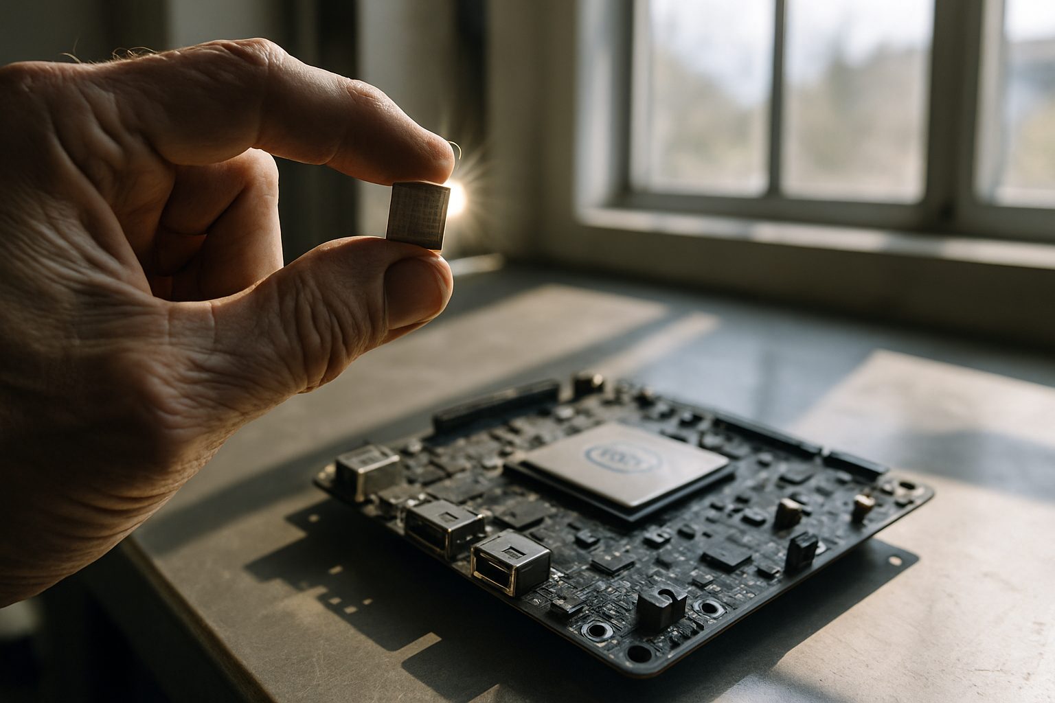
TL;DR: Waymo unveiled a 5nm custom ML ASIC delivering 1,000+ TOPS to process sensor data in milliseconds, replacing Intel FPGAs. The move reflects competitive pressure from Tesla and signals that AV-grade silicon is becoming a core differentiator rather than commodity hardware.
The Strategic Implication: Custom Silicon Now Table Stakes for AV Leaders
Waymo’s shift from FPGAs to purpose-built silicon isn’t incremental engineering—it’s a competitive moat in hardware. By moving perception and decision-making latency from tens of milliseconds to near-instantaneous response, Waymo raises the bar for any competitor relying on off-the-shelf accelerators. For investors, this signals that autonomous vehicle advantage increasingly concentrates in companies that control their silicon stack.
The timing matters. According to The Register’s reporting, Waymo’s ASIC rollout comes as Tesla accelerates its own chip development, turning compute architecture into a direct competitive battleground.
Technical Specifications and Redundancy Architecture
Raw Performance Metrics
Built on TSMC’s 5nm process, Waymo’s chip claims 1,000+ TOPS for AI workloads. The design incorporates both classical CNNs and transformer-based models, processing data from 12+ onboard cameras. The company trained the silicon on 200+ million miles of autonomous driving data to optimize decision accuracy.
The TOPS figure likely represents INT8 precision—placing it in the same performance class as Nvidia’s Drive AGX Thor but with custom optimization for AV-specific inference patterns.
Latency-Critical Redundancy
Each vehicle runs dual ASICs operating as a single compute unit under normal conditions. If one chip fails or returns an erroneous result, the second seamlessly takes over. This N+1 architecture mirrors fault-tolerance strategies in aerospace, where a third system can serve as tiebreaker logic.
Thermal management runs through liquid cooling integrated with vehicle coolant systems, maintaining optimal operating temperatures across extreme temperature swings—a datacenter problem Waymo solved through vehicle-level hardware integration.
Why Custom ASICs Beat FPGAs for Autonomous Driving
Waymo previously deployed Intel FPGAs for sensor processing. While FPGAs excel at low-latency applications (high-frequency trading uses them for this reason), they impose steep programming complexity and deliver lower compute density than dedicated silicon.
- Compute density: ASICs pack more transistors per mm² than reconfigurable logic
- Power efficiency: Purpose-built dataflow reduces wasted computation
- Latency predictability: Fixed hardware pathways guarantee response times within milliseconds
- Scalability: Designing once at 5nm amortizes R&D across fleet deployments
In autonomous driving, milliseconds determine safety outcomes. A car traveling at 60 mph covers 88 feet per second; a 50ms decision delay spans 7+ feet—the difference between collision and evasion.
Background: The AV Chip Race Intensifies
Waymo, Alphabet’s autonomous vehicle subsidiary, has operated robotaxi services in Phoenix, San Francisco, and Los Angeles. The company competes directly with Tesla’s Full Self-Driving stack and emerging autonomous vehicle startups. Waymo’s move to custom silicon reflects both technical necessity and competitive differentiation—the company cannot afford to rely on Nvidia’s public architectures when Tesla designs its own.
Tesla’s chip program has accelerated under Elon Musk’s leadership, with engineers like Jim Keller pushing custom silicon for FSD compute. Tesla manufactures vehicles with its own inference accelerators, giving the company vertical integration Waymo must now match to remain competitive in the robotaxi market.
TSMC’s 5nm node represents the current frontier for mobile and edge AI inference. At this process node, power efficiency (TOPS per watt) becomes the limiting factor in thermal budget-constrained applications like vehicles. Waymo’s choice of 5nm signals aggressive performance targets—likely drawing 20-50W for the dual-chip setup.
Broader industry context: Custom ASICs for autonomous systems are no longer exotic. Mobileye (Intel subsidiary) uses custom inference accelerators; Qualcomm developed Snapdragon Ride; Nvidia continues optimizing Drive Orin for OEM integration. Waymo’s ASIC represents the continuation of a three-year trend toward proprietary silicon in Level 4 autonomy stacks.
What This Means for the AV Industry
Waymo’s ASIC design validates a uncomfortable truth: off-the-shelf GPU/accelerator platforms cannot meet the latency, reliability, and redundancy demands of production autonomous vehicles. Every serious AV competitor now faces a build-versus-buy decision.
For Tesla, this removes competitive pressure from Nvidia and validates its in-house chip strategy. For Waymo and other Level 4 startups, custom silicon becomes a mandatory R&D investment—increasing the capital required to reach production autonomy and tilting advantage toward well-funded players.
The real competition isn’t TOPS anymore. It’s milliseconds, redundancy layers, and thermal integration. Waymo just raised the ante.
About the Author